
Abstract
MEMS devices play an important role in modern technologies, including computers, medical devices, and chemical engineering. This high demand for MEMS devices drives the need for effective fabrication processes, which utilize semiconductor manufacturing principles to produce high-quality MEMS devices. Through applying standard semiconductor manufacturing techniques, including photolithography, etching and deposition to a particular type of MEMS device — MEMS Microvalve, this paper theoretically proposed a step-by-step procedure for fabricating MEMS Microvalve. The microvalve is customized to enable liquid-level detection, and is applied here in developing a MEMS-based gasoline shortage detector that could be used in modern vehicles. Through past relevant papers, this paper also presents the rationale behind the chosen methodology and materials chosen for the fabrication process of the microvalve.
Keywords: MEMS, microvalve, semiconductor manufacturing, methodology, gasoline shortage detection, application
Introduction
MEMS, which stands for micro-electromechanical systems, are crucial components of modern electronics, particularly in detection, sensing and actuating. These miniature devices integrate mechanical elements, actuators, sensors, transducers, and electronics onto a single chip, and can be applied in various applications, such as airbag sensors in cars, blood pressure monitors, optical sensors, and computers1. They not only have small size, but also allow for minimal energy consumption, reducing device costs while enabling substantial information processing. Due to these advantages, this paper will seek the theoretical possibility of applying MEMS microvalve in sensing whether the vehicle is experiencing a gasoline shortage. MEMS-based gasoline shortage detector uses the MEMS microvalve structure to convert physical signals into electric signals, which better meets the demand for digitalization and miniaturization of modern vehicles than traditional float sensors.
The high complexity and demand for MEMS devices in the industry necessitates efficient and precise manufacturing techniques. To develop MEMS devices, it is essential to not only understand their functionality, but also their manufacturing process2‘3. The structure of MEMS is generally built upon a polished silicon wafer, and undergoes repeated sequences of photolithography, etching, and deposition, along with additional steps, like doping, ion implantation, metallization, passivation, and packaging. These processes must be conducted in a highly dust-free cleanroom, with processors in specialized bunny suits to avoid contaminating the processing wafer. Given the strict lab requirements of semiconductor cleanroom, this study is positioned as a preliminary design proposal which provides a theoretical framework and structural basis for MEMS microvalve devices, and its application in gasoline shortage detection. Future experiments are proposed in Section 6 to evaluate the device’s feasibility and performance.
Classical Semiconductor Fabrication Techniques
In this section, classical semiconductor fabrication techniques are introduced.
Crystal Growth and Wafer Preparation
Crystal growth is the initial step of semiconductor manufacturing. In industry, this step is typically achieved by using the Czochralski method2. This crystal growth technology involves inserting a small seed crystal into a melted crucible of high-purity silicon, then pulling out and cooled to zero degrees Celsius to obtain a single crystal of semiconductor. The crystal is then sliced into thin slices, which are then polished and cleaned into silicon wafers that are ready to use.
The wafer-cleaning process is also a crucial step for ensuring a defect-free surface4‘5. This process helps prepare a wafer surface free of metallic, particulate, and organic contaminants while ensuring the wafer surface or substrate remains undamaged.
Oxidation
Oxidation provides an insulation layer that isolates the silicon substrate from the conductive material6. Silicon dioxide is the primary inorganic material used in the industry, which is one of the principal reasons for silicon’s dominance in the integrated circuit industry2. There are a couple of main reasons why silicon dioxide is widely used. First, it is easily selectively etched using lithography. Secondly, it can mask most of the common impurities, such as boron (B), phosphorus (P), arsenic (As), and antimony (Sb). Moreover, it is an excellent insulator that has stable electrical properties. Finally, it has a stable and reproducible interface with silicon.
The primary method of depositing the SiO2 insulation layer is thermal oxidation, as it provides a conformal oxide film of uniform thickness6. The process of thermal oxidation involves introducing pure oxygen or water vapor into high-temperature furnaces to react with the silicon substrate, which results in the formation of silicon dioxide7. As the process proceeds and the oxide layer grows thicker, the oxygen must get through the already-grown oxide to react with the silicon. This means the freshest layer of oxide is always at the interface, which can allow you to get a very high-quality interface there, as contaminants from the starting substrate will be consumed by the top layer of grown oxide.
Deposition
Deposition is the process of depositing a thin film of material on a substrate2. Metal and dielectric layers, such as Au-Ti bilayer, are typically deposited to interconnect devices on the wafer7. Conformal coating is also a common deposited layer in semiconductor fabrication to protect the device from the external environment. Parylene, in particular, is a widely used conformal coating that prevents device damage from hydrocarbon fluids, such as fuels.
The key metrics of deposition are material crystallinity (such as single crystal, polycrystal, and amorphous), deposition rate, controllability, conformality, and uniformity. Material crystallinity is important because the material structures of the deposition layers can influence the performance of the wafer. The deposition rate is a metric that is crafted for each device because of the different thicknesses desired. The ability to control the process is also a key metric as it is important to deposit the same thickness every time. Additionally, when fins and multiple gates are needed, it is essential to deposit conformally. Finally, being able to deposit uniformly on the entire wafer is crucial for the yield of the chips produced from a single wafer.
The main deposition methods are Physical Vapor Deposition (PVD), Chemical Vapor Deposition (CVD), and Atomic Layer Deposition (ALD)2. PVD involves heating a piece of metal on a heating strip, which vaporizes the metal and therefore forms a thin layer of metal on the wafer. CVD includes two main types: Plasma Enhanced Chemical Vapor Deposition (PECVD) and Metal Organic Chemical Vapor Deposition (MOCVD). In PECVD, a wafer placed inside a vacuum chamber with plasma is exposed to vaporized sources flowing through the chamber continuously. These sources will then diffuse and react on the wafer surface, leading to the deposition when enough energy is reached. MOCVD is a process used to deposit compound materials at near-atmospheric pressure8. This is a versatile technique that is able to control the various thermal dynamic interactions, offer high deposition rates, large area uniformity, and an effective doping process9. ALD is a layer-by-layer process that deposits one layer of atoms at a time10‘11. Each layer is formed by a saturated self-controlled surface reaction between the substrate and precursor molecules. Because of this, ALD offers an advantage over PVD by providing conformal, thickness-controlled, and uniform thin film deposition. However, the process of ALD can be costly and slow when depositing thicker layers. Therefore, ALD is normally used to deposit extremely thin layers, sometimes only a few atoms thick, such as the Al2O3, which can serve as an adhesion interface between A-174 silane and parylene.
Photolithography and Patterning
Photolithography is a key step in semiconductor manufacturing12‘13. It is a technique for transferring geometric patterns from a mask onto the surface of a wafer or substrate14. Firstly, substrate material and geometry are selected, typically a 4”-8” single-crystal wafer2. Secondly, the wafer is coated with a layer of photosensitive polymer, called a photoresist. Then, it is exposed to ultraviolet light with a precisely patterned mask, a fused silica (quartz) plate designed from software, where a certain region will become soluble. When immersed in solution (developer), either exposed regions (positive process) or unexposed regions (negative process) will be chemically removed. After this, the wafer will be dried, and the photoresist is used as a mask for ion implantation, barrier formation, deposition, or etching.
Etching
Etching is the selective removal of a particular thin film from certain locations on the wafer surface7‘2. The locations to be eliminated are identified using a “mask” film, which can be photoresist or another type of thin film. In general, there are various ways to etch a given thin film, however, the chosen method is dependent on the required etching condition. The choice of etch process can be determined by several key factors, such as, the speed of the removal of the material (etch rate), and the etch profile. Normally, the anisotropic etch profile is preferred, as this only etches the material in one direction, so there won’t be an undercut as the isotropic etch profile will. Additionally, uniformity is also greatly considered, as it is essential to etch the entire surface uniformly. Finally, selectivity determines whether the materials can be etched effectively without damaging other parts of the locations.
As the primary etching method in advanced wafer fabrication, dry etching is an anisotropic etching process, which is a process that selectively removes materials only in one direction. This gives the advantage of being able to etch sharp corners, flat surfaces, and deep cavities. However, the disadvantage is that dry etching has low selectivity which can cause damage to wanted areas. An important type of dry plasma reactor is Reactive Ion Etching (RIE). During this process, ions are shot through the plasma sheath around the mask to “dig” out unwanted areas. A typical process uses SF₆/O₂ to etch the wafer. SF₆ breaks down the plasma and releases fluorine radicals15. Then these radicals reacts with the silicon and forms SiF₄, which gets pumped away. O₂ reacts with the silicon to form a SiOₓ passivation film on the sidewalls, which slows down lateral etching. CHF₃ is sometimes added to enhance the passivation layer, as it can deposit polymers on the sidewalls. Normally the etch rate of RIE is 0.05-0.6 μm/min depending on the power of RF and the mixture of gases.
In contrast to dry etching, wet etching is an isotropic etching process, where chemical reactions occur to etch around the mask. This process has very high selectivities as this process is completely chemical, However, this process etches isotropically in all directions, which could cause patterns to collapse.
In general, wafer preparation, oxidation, deposition, etching, photolithography and patterning form the foundation of MEMS fabrication. The objective of this paper is to explore how to apply these methods to propose a fabrication process of a MEMS microvalve, as well as adapting the methods and materials chosen for the device to be able to perform gasoline sensing. This paper will include a step-by-step fabrication process of this device, rationales for selected fabrication method, thickness and material of each layer, as well as the application of the microvalve as a gasoline shortage detector.
Method
A comprehensive literature review on semiconductor manufacturing key processes, including wafer preparation, oxidation, deposition, etching, and photolithography, is conducted through summarizing, analysing, and organizing academic papers, books and Purdue University’s “Semiconductor Fabrication 101 Course”. Academic papers referenced are obtained through three key databases: Google Scholar, ScienceDirect, and IEEE. Some search keywords used are: “Semiconductor Manufacturing”, “MEMS Fabrication”, “MEMS Microvalve”. To narrow down to specifics of each technique or materials used, keywords like “Atomic Layer Deposition”, “parylene coating”, “reactive ion etching”, and “parylene and hydrocarbon solvent” are used.
Selection criteria of fabrication technique is based on the consideration of the pros and cons of each fabrication technique, such as anisotropy, conformality, and thermal compatibility with the material and structure. For example, Reactive Ion Etching (dry etching) is chosen in etching the silicon wafer in Figure 3, due to the anisotropic nature of dry etching2. PVD is chosen to deposit Au-Ti bilayer (Figure 7), due to its significant advantage in depositing metals, such as uniformity, low-contamination and low-temperature deposition2.
Design parameters, including layer thickness, etching depth, and gap width, are theoretically derived from documented experimental data in previous microvalve studies and standard semiconductor fabrication references. These data are derived through consideration of mechanical flexibility, electrostatic properties, and chemical resistance etc. For example, a device layer of 15 μm is chosen based on the optimal thickness for RIE, the etch rate for the silicon layer is chosen based on the optimal etch rate experimented under optimized conditions in Legtenberg et al.15.
Results
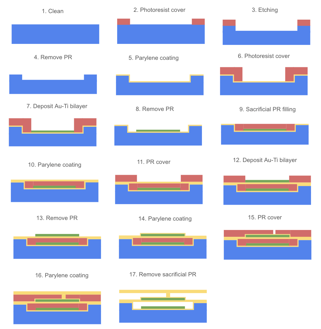
The fabrication process of the MEMS microvalve begins with a double side polished 4” or 6” silicon wafer, with a device layer 15 μm thick, an oxide layer 1 μm thick, and a substrate that is 500 μm thick (Figure 1). Then the wafer can be cleaned by the piranha solution16‘17. The optimal silicon thickness for RIE is in the range of 10 – 20 μm depending on the O₂/SF₆ ratio15. Therefore, a thickness of 15 μm is chosen in this design as it is a good balance between mechanical flexibility for valve actuation and sufficient thickness to minimize stress. However, experimental validation is required to determine the optimal thickness in the long term.
Then, two photoresist layers, each about 10 μm wide, are deposited onto both ends of the wafer to protect the areas from being etched (Figure 2). This is followed by reactive ion etching (RIE) to etch about 4 μm deep into the silicon wafer at a rate of approximately 0.5 μm/min with SF₆/O₂ (Figure 3). This choice of dry etching (RIE) is due to its anisotropic nature2. This method gives the substrate a flat surface, which is more beneficial for the following steps of building the dielectric and electrode layers on top of the substrate.
Photoresist is then removed by dry plasma ashing (Figure 4). Dry plasma ashing with oxygen is the standard method to remove photoresists today7‘18‘19. Because it is efficient and leaves minimal residue compared to solvent-based stripping. However, this process involves both chemical reactions and physical bombardment by ions, which can oxidize polymers and break polymer chains, causing damage to the parylene layer. Although oxygen plasma ashing remains the chosen method in this design, steps where the parylene layer is exposed require special control, such as low RF and shorter exposure time.
After that, a thin parylene coating (about 1 μm thick) is deposited onto the surface of the etched silicon wafer by CVD to insulate materials (Figure 5). As a typical organic insulator, parylene coating can separate materials throughout the process20. Due to its high conformality and having a deposition temperature near room temperature6, this layer not only protects the device from the environment, such as dust, temperature, and moisture, but also acts as a dielectric that separates the electrodes, which prevents a short circuit21. CVD is often chosen to deposit Parylene because it is the only deposition method to turn parylene dimer into polymer film. Unlike PVD, CVD can ensure the coat is highly conformal, especially on the sidewalls. Although ALD is also able to deposit conformal films, it is costly and impractical to deposit micron-thick layers10‘11. Additionally, the optimal parylene thickness needs to be verified as described in section 6.
The surface is then covered with photoresist 16 μm from either end of the substrate to mask these areas during deposition (Figure 6). An Au-Ti bilayer about 2 μm thick is proposed to coat the middle portion of the wafer (Figure 7). As a heterogeneous material, the Au-Ti bilayer has different thermal and mechanical parameters on both sides, which can trigger highly effective hot electron transfer when combined with semiconductors22. Due to the outstanding electrical conductivity of Au and strong bonding of Ti to the oxide substrate, Au-Ti bilayer is widely used as an electrode in electronic devices7. PVD is normally chosen to deposit the Au-Ti bilayer. Because unlike CVD and ALD, PVD enables the metal layers to be stacked more quickly with low contamination and good uniformity. Additionally, PVD can happen at room temperature, which lowers the risk of damaging the underlying oxide layer. In MEMS fabrication, metal electrodes and interconnection films typically range from a few hundred nanometers to a few microns in thickness23. Increasing sheet thickness reduces sheet resistance and improves film durability. Therefore, the Au-Ti bilayer thickness in this design is set to be 2 μm which is in this reasonable range, although experiments or simulations would be required to find the optimal thickness in long-term performance described in section 6.
Subsequently, photoresist is removed by dry plasma ashing to expose the Parylene coated areas (Figure 8). The middle gap is then filled with sacrificial photoresist to align its height with the parylene coated level on both sides (Figure 9). A thin layer of Parylene F coating, approximately 2μm thick, is deposited onto the surface by CVD at room temperature (Figure 10). Parylene F (fluorinated parylene) is chosen to be deposited onto this surface to increase device resistance, as it will come into contact with gasoline.
The surface from either end of the substrate is covered with approximately 16 μm photoresist to mask these areas during the deposition of Au-Ti bilayer (Figure 11). After that, an Au-Ti bilayer about 2 μm thick is deposited onto the surface in between the photoresists on either end (Figure 12). The photoresist is then removed by dry plasma ashing to expose the parylene surface (Figure 13).
To protect the metal layer from contact with gasoline, a thin layer of Parylene F coating approximately 1 μm thick is deposited onto the surface (Figure 14). A sacrificial photoresist about 28 μm from the left end of the substrate and another sacrificial photoresist 22 μm from the right end of the substrate are deposited, leaving a 4 μm gap in between (Figure 15). Both sacrificial photoresists are about 6 μm thick. These layers are deposited to create a defined space between the structures. A Parylene F coating about 3μm thick is subsequently deposited to fill the gap and cover the top of the photoresist to create a channel where gasoline can flow through (Figure 16). And all the sacrificial photoresists are removed by dry plasma ashing to reveal the valves and spaces in between the structures (Figure 17).
Lastly, to protect the structure, the wafer undergoes Wafer-Level Packaging (WLP) and is then diced. WLP is commonly used to encapsulate the MEMS devices24. First a capping wafer is fabricated by etching through-holes for fluid inlet and outlet. Then the cap wafer is accurately aligned with the original wafer where hermetic bonding is performed to seal the structure. Lastly, the bonded wafer is diced into individual chips.
Discussion
This microvalve device can be applied as a gasoline sensor in automobiles. It can be placed on the side of the fuel tank at a certain height above the bottom of the tank to detect the fuel level. When the fuel level is above the preset height, gasoline fluids enter the valve and exerts pressure to the compliant Parylene-coated diaphragm, which causes it to deflect and closes the opening in between. On the contrary, if it is below, the diaphragm reopens and triggers the signal light which alerts the driver that the vehicle is low on gas. However, this must only happen when the vehicle is moving on a flat surface. With that said, this sensor must be connected to a gyroscope, which is a separate device from the microvalve connected within the system. The signal light should only light up when the vehicle is not tilted and the microvalve is open to let the driver know the vehicle needs gas. By implementing a logic configuration, specifically an AND gate, this circuit level integration can be realized using standard CMOS (complementary metal–oxide–semiconductor) circuitry7.
The advantages of this MEMS-based sensor system over traditional float sensors are that it is more precise and more reliable, the integration of gyroscope and logic gates are less likely to give false alerts. Additionally, the small size can be easily integrated into compact systems and potentially reduce the cost. The table below provides a more detailed comparison:
| | Traditional Float Sensors | MEMS |
| Size | 6 x 2.7 x 5.1 inches25 | Small – on a mm-scaled chip (for example, a type of thermopneumatic microvalve has a size of 7.5 × 10.3 × 1.5 mm^3)26 |
| Cost (estimated) | $25-$25027 | $1-$528 |
| Accuracy | ±1-5%29 | Normally high accuracy, future experiment is needed to determine the accuracy of MEMS microvalve in gasoline sensing26 |
| Response Time | Normally in seconds | Very fast – on the ms scale |
| Temperature Range | Up to 185 ℉30 | A typical microvalve could function normally at 80-380 K (-316 ℉ – 224 ℉)31 |
The limitation of this design might be device inaccuracy caused by gasoline’s viscosity. Although gasoline has a lower viscosity (0.6 centipoise) than water (1 centipoise), it’s higher than typical gases, such as air which is only about 0.018 centipoise32‘33. The high viscosity of the fluid might cause droplets to get stuck on the sidewalls of the microvalve; therefore, it may not be able to trigger the signal light when the vehicle is low on gas.
Parylene F is deposited for layers that are exposed to gasoline to increase the device’s resistance in an automobile environment. Due to the strong C-F bond (485 kJ/mol), Parylene F is generally more resistant to chemicals than Parylene C34. Additionally, Parylene F has high temperature and UV resistance35. These properties ensure the stability of the material in an automobile environment. However, using Parylene F in the design comes with trade-offs, such as higher cost due to a more complex deposition process, and the possible need for an adhesion promoter. Additionally, it is unclear whether Parylene F reduces the likelihood of hydrocarbon droplets adhering to the microvalve sidewalls. A proposed experimental design to address this limitation is described in the next section.
Another potential limitation in this design is the internal stress within parylene. As a polymer, parylene can build up internal stress with the increase of thickness and the number of the layers, which could cause cracking and delamination under thermal or mechanical stress. One way to reduce the impact of this is to deposit a thin layer of Al2O3 by ALD, followed by a layer of A-174 silane adhesion promoter before the deposition of parylene36. This provides a chemically bonded interface between parylene and the substrate, improving the device’s resilience to stress. However, additional thermal cycling tests are necessary to verify whether this adhesion method can withstand repeated expansion and contraction in the automotive environment.
The unknown long-term performance of the device is also a limitation of this study. The environment in an automobile involves vibration, frequent temperature changes, and prolonged contact with gasoline. Although this design incorporates a protective layer (Parylene F coating), an adhesion promoter (A-174 silane) and wafer-level packaging, experiments are necessary to evaluate the device’s durability under conditions that imitate a practical automobile environment. In addition, yield and cost analyses are essential to determine whether the process is scalable for mass production.
The expectation for future microvalves is to lower the voltage required to operate, achieve faster valve actuation, and increase seating pressure to reduce leakage5‘37‘26. Currently, the most effective types of valves with high actuation rates are piezoelectric and electromagnetic valves38‘39. However, increasing the seating pressure in an electromagnetic valve requires a higher voltage because more force is needed to overcome the higher pressure. This presents a challenge, as higher voltage can lead to increased power consumption and potential overheating. Therefore, future research must focus on developing innovative solutions to enhance electromagnetic valve performance without necessitating higher voltages.
The expected operational voltage of this electrostatic microvalve is between 50-110V, and the input pressure can be up to 40 kPa17. Research shows that this type of microvalves can respond as fast as 50 µs and can be opened and closed up to 47,000,000 times before failure17. Since gasoline pressure in fuel tanks is quite low, the sensitivity of this microvalve for liquid sensing can be low, as typical applied pressure of the fluid for microvalves range from a few kPa up to hundreds of kPa40. Additionally, a typical microvalve can operate in the temperature range 80 – 380 K17. However, experimental validation is required to establish more accurate estimates for this device.
Future Validation Methodology
Given that this study is positioned as a preliminary design proposal, a comprehensive validation methodology is described below to verify the feasibility and performance of the proposed design of MEMS microvalve.
Micro-Scale Simulation
Using COMSOL Multiphysics software or ANSYS Student, finite element analysis (FEA) simulations can be conducted to test out the functionality of the device computationally and make adjustments accordingly before experimenting in the cleanroom. There are three key simulations:
- Fluid Pressure Simulation. This is to model the pressure gasoline creates at low fuel level and predict the pressure required to open the membrane.
- Membrane Deflection Simulation. This is to evaluate the diaphragm deflection under gasoline pressure and whether the chosen membrane thickness can avoid permanent deformation
- Flow Simulation. This is to analyze whether liquid viscosity and surface adhesion affects valve closure.
- Layer Thickness Simulations. The thickness of the Au-Ti bilayer needs to undergo electrical, mechanical, and thermal simulations to verify the optimal thickness for this device. FEA simulations will test Au-Ti bilayer from a range of 0.2 – 4 µm, and compare sheet resistance, residual stress and thermal expansion mismatch to find the optimal thickness. In addition to Au-Ti bilayer, simulations will also verify mechanical stability and functional requirements of other thicknesses, such as the 1-3 µm Parylene coatings, the 6 µm sacrificial photoresist layers and the 4 µm RIE etch depth.
Material Testing
After completing the computation simulation, the materials chosen will be tested for chemical and thermal resistance. Experiments are as follows:
- Parylene F and Parylene C Gasoline-Exposure Testing: Both Parylene F and Parylene C test strips 12-35 microns thick will be submerged to gasoline under different temperatures that mimic automobile environments35. Measure and compare their percentage of swelling.
- Hydrocarbon Droplet Adhesion Testing on Parylene F and Parylene C: To evaluate whether gasoline droplets would be less likely to stick to the sidewalls, standard sliding-angle test can be conducted. A small droplet of hydrocarbon liquid is placed on two coated test strips, one coated with Parylene F and another with Parylene C. Then the test strips are slowly tilted until the droplets begin to move. Compare the tilt angle of the two test strips. A lower tilt angle indicates lower droplet adhesion and reduced likelihood of droplets getting stuck on the microvalve sidewalls.
- Adhesion testing with A-174 silane: Two sets of test samples are compared with one coated with Parylene F directly and another coated with A-174 silane and Parylene F deposited on top. Both sets will undergo identical thermal cycling tests that simulate temperature fluctuation inside a vehicle environment. After thermal cycling, adhesion strength will be assessed using standard peel-test and scratch-test.
Microfabrication testing
After the more optimized materials are chosen and verified, the microfabrication methods will be tested. Experiments are as follows:
- RIE Etch Rate and Etch Depth Testing: Use a profilometer to measure the step height between the etched region and the unetched region to verify whether the expected 4 µm etch depth and the 0.5 µm/min etch rate are met.
- Au-Ti Bilayer Thickness and Uniformity Testing: Use a profilometer to measure the metal thickness to ensure the electrode layer is neither too thick nor too thin. Then use a four-point probe to measure the sheet resistance to confirm its electrical performance. Lastly, an optical microscope is used to check for cracks and delamination.
- Parylene C and Parylene F Thickness Testing: Similarly, the thickness of the parylene layers will be verified using a profilometer. Additionally, cross-section SEM can also be used to check the sidewall coverage and the uniformity of the Parylene layers.
- Sacrificial Photoresist Thickness and Channel Height Testing: Before the removal of photoresist, the thickness of it will be measured with a profilometer. Then after removal, an optical microscope can be utilized to check whether the final channel is open and whether there are defects on the channel surface.
Long-term reliability Testing
A series of tests will be performed to mimic an accelerated vehicle environment to evaluate the mechanical, chemical and thermal stability of the device.
- Accelerated Thermal Cycling
This simulation is done by placing the device into a temperature controlled chamber to mimic the temperature environment of an automobile. Control the chamber temperature so that it cycles between -20 °C to + 80 °C and hold each temperature for approximately 10 minutes. Repeat this cycle 200-300 cycles to mimic the long term use of the device. Then, check for cracking, delamination and shape changes of the membrane shape with an optical microscope.
- Accelerated Chemical Soaking
This test evaluated the device’s chemical resistance in gasoline. A packaged device will be soaked in gasoline solution under a fume hood and then dried in 1 hour intervals. This process will be repeated for 40 cycles. After the device is dried and cooled to room temperature for each cycle, electrical conductivity, valve function (open and close), and sliding angle will be tested and recorded. Additionally, a profilometer will also be used to check for swelling of any surface.
- Accelerated Mechanical Cycling
A Peristaltic pump will be used to open and close the microvalve repeatedly to check for mechanical fatigue and failure. The valve will undergo 5000-10000 cycles while monitoring the diaphragm performance and whether the electrical circuit opens and closes consistently in sync with the position of the microvalve. After the cycling test, cracks and delaminations are checked under an optical microscope.
Conclusion
This paper presented how the principles of semiconductors could be applied in the fabrication process of MEMS devices and how MEMS microvalve could be applied in gasoline level detection. The introduction section provided an overview of MEMS devices and general steps in the fabrication process. The literature review section described each step in detail with different methods used in the fabrication process, and the advantages and disadvantages. A step-by-step fabrication process along with the selected materials for a microvalve MEMS device was proposed in the Result section. The Discussion section explained practical application of the device in detecting gasoline shortage in automobiles, justification for the methods and materials chosen, as well as limitations of the paper. Finally, the Future Validation Methodology section presented a set of proposed experiments to validate this preliminary design.
References
- Analysis and design principles of MEMS devices. (n.d.). Google Books. https://books.google.com/books?hl=en&lr=&id=No7NNfc1pfYC&oi=fnd&pg=PP1&dq=mems+device&ots=whzopk1Osv&sig=XwVKf_TyQ1szJGZ-coMfEJbeZng#v=onepage&q=mems%20device&f=false [↩]
- Purdue University, the University of Texas at Auston, ASML, Penn State University, “Semiconductor Fabrication 101 Course,” Available: https://purdue.brightspace.com/d2l/le/content/984062/viewContent/14739830/View [↩] [↩] [↩] [↩] [↩] [↩] [↩] [↩] [↩] [↩]
- Qu, H. (2016). CMOS MEMS fabrication technologies and Devices. Micromachines, 7(1), 14. https://doi.org/10.3390/mi7010014 [↩]
- Bera, B. (2019b). Silicon wafer cleaning: a fundamental and critical step in semiconductor fabrication process. In International Journal of Applied Nanotechnology (Vols. 5–5, Issue 1, pp. 8–13). JournalsPub. https://www.static-contents.youth4work.com/y4w/fc469004-19c4-4401-81ce-90d5c073564d.pdf [↩]
- Ju, B., Wang, Q., Fang, L., Liu, F., Li, G., & Liu, Y. (2021). Single-layer piezoelectric transformers with a unique design of polarization topologies. Sensors and Actuators a Physical, 332, 113193. https://doi.org/10.1016/j.sna.2021.113193 [↩] [↩]
- Dixit, P., & Henttinen, K. (2015). Via technologies for MEMS. In Elsevier eBooks (pp. 694–712). https://doi.org/10.1016/b978-0-323-29965-7.00038-5 [↩] [↩] [↩]
- Quirk, M., & Serda, J. (n.d.). Semiconductor manufacturing Technology. Prentice Hall. https://su2al.com/IAGblog/wp-content/uploads/2010/07/Semiconductor-Manufacturing.pdf [↩] [↩] [↩] [↩] [↩] [↩]
- Dapkus, P. D., Chi, C. Y., Choi, S. J., Chu, H. J., Dreiske, M., Li, R., Lin, Y., Nakajima, Y., Ren, D., Stevenson, R., Yao, M., Yeh, T. W., & Zhao, H. (2020). Selective area epitaxy by metalorganic chemical vapor deposition– a tool for photonic and novel nanostructure integration. Progress in Quantum Electronics, 75, 100304. https://doi.org/10.1016/j.pquantelec.2020.100304 [↩]
- Lu, Y., Shi, Z., Shan, C., & Shen, D. (2019). ZnO nanostructures and lasers. In Elsevier eBooks (pp. 75–108). https://doi.org/10.1016/b978-0-12-814162-5.00004-2 [↩]
- ASM. (n.d.). ALD (Atomic Layer Deposition) | ASM. https://www.asm.com/our-technology-products/ald [↩] [↩]
- Ovanesyan, R. A., Filatova, E. A., Elliott, S. D., Hausmann, D. M., Smith, D. C., & Agarwal, S. (2019). Atomic layer deposition of silicon-based dielectrics for semiconductor manufacturing: Current status and future outlook. Journal of Vacuum Science & Technology a Vacuum Surfaces and Films, 37(6). https://doi.org/10.1116/1.5113631 [↩] [↩]
- Lin, B. J. (2004). Immersion lithography and its impact on semiconductor manufacturing. Journal of Micro/Nanolithography MEMS and MOEMS, 3(3), 377. https://doi.org/10.1117/1.1756917 [↩]
- Control of lithography in semiconductor manufacturing. (2006, December 1). IEEE Journals & Magazine | IEEE Xplore. https://ieeexplore.ieee.org/abstract/document/4019321?casa_token=ZvdCvStFfMMAAAAA:tHwtm9PIMciiDDNy6Nxl7if1gaFz1lsEJNq3RIu4S6EUPam9hDIAeqcezHBo3O6YwxQH5Mu_VBc [↩]
- Yap, F., & Zhang, Y. (2006). Protein and cell micropatterning and its integration with micro/nanoparticles assembly. Biosensors and Bioelectronics, 22(6), 775–788. https://doi.org/10.1016/j.bios.2006.03.016 [↩]
- Legtenberg, R., Jansen, H., De Boer, M., & Elwenspoek, M. (1995). Anisotropic reactive ion etching of silicon using SF 6 / O 2 / CHF 3 gas mixtures. Journal of the Electrochemical Society, 142(6), 2020–2028. https://doi.org/10.1149/1.2044234 [↩] [↩] [↩]
- Yıldırım, E., Arıkan, M. S., & Külah, H. (2012). A normally closed electrostatic parylene microvalve for micro total analysis systems. Sensors and Actuators a Physical, 181, 81–86. https://doi.org/10.1016/j.sna.2012.05.008 [↩]
- Qian, J., Hou, C., Li, X., & Jin, Z. (2020). Actuation Mechanism of Microvalves: a review. Micromachines, 11(2), 172. https://doi.org/10.3390/mi11020172 [↩] [↩] [↩] [↩]
- Resist Removal | Stanford Nanofabrication Facility. (n.d.). https://snfguide.stanford.edu/guide/equipment/purpose/cleaning/resist-removal [↩]
- Parylene etching techniques for microfluidics and bioMEMS. (2005). IEEE Conference Publication | IEEE Xplore. https://ieeexplore.ieee.org/stamp/stamp.jsp?arnumber=1453993 [↩]
- Coating, A. (n.d.). Why Parylene conformal coating? | Advanced coating. https://www.advancedcoating.com/why-parylene#:~:text=A%20parylene%20conformal%20coating%20is,%2C%20mechanical%20forces%2C%20or%20chemicals [↩]
- Anjewierden, D., Liddiard, G. A., & Gale, B. K. (2012). An electrostatic microvalve for pneumatic control of microfluidic systems. Journal of Micromechanics and Microengineering, 22(2), 025019. https://doi.org/10.1088/0960-1317/22/2/025019 [↩]
- Lian, Y., Jiang, L., Sun, J., Tao, W., Chen, Z., Lin, G., Ning, Z., & Ye, M. (2023). Ultrafast dynamics and ablation mechanism in femtosecond laser irradiated Au/Ti bilayer systems. Nanophotonics, 12(24), 4461–4473. https://doi.org/10.1515/nanoph-2023-0497 [↩]
- Thin Films – microfab – MEMS Manufactory. (2021b, May 7). Microfab – MEMS Manufactory. https://microfab.de/fabrication-services/thin-films/ [↩]
- Bleiker, S., Taklo, M. V., Lietaer, N., Vogl, A., Bakke, T., & Niklaus, F. (2016). Cost-Efficient Wafer-Level capping for MEMS and imaging sensors by adhesive wafer bonding. Micromachines, 7(10), 192. https://doi.org/10.3390/mi7100192 [↩]
- Amazon.com. (n.d.). Sending Units 240-33 marine vehicle fuel level sender [Product page]. Amazon.com. https://www.amazon.com/Sending-240-33-Marine-Vehicle-Sender/dp/B092MVF5 [↩]
- Hsu, C. J., & Chen, K. H. (2020). “Advancements in Microvalve Technologies: A Comprehensive Review on Actuation Mechanisms and Performance Metrics.” Journal of Micromechanics and Microengineering, 30(11), 113002. doi:10.1088/1361-6439/abb074 [↩] [↩] [↩]
- Fuel level sensors. (n.d.). AutoZone. https://www.autozone.com/engine-management/sensor-fuel-level [↩]
- Buy MEMS and sensors – eStore – STMicroelectronics | Page 2. (n.d.). https://estore.st.com/en/products/mems-and-sensors-page2.html [↩]
- Level sensor devices vs. traditional methods: Which is more accurate and efficient? (2025, January 20). Rika Sensor. https://www.rikasensor.com/a-level-sensor-devices-vs-traditional-methods-which-is-more-accurate-and-efficient.html#:~:text=Accuracy%20Comparison:%20%2D%20Traditional%20Methods:%20Float%20and,sensors%20can%20achieve%20accuracies%20up%20to%20%C2%B10.2%25. [↩]
- Smith, F. J. & Madison Company. (n.d.). Continuous Level Float sensors. https://cdn.thomasnet.com/ccp/00472059/35768.pdf [↩]
- Park, J. M., Brosten, T. R., Evans, A. T., Rasmussen, K., Nellis, G. F., Klein, S. A., Feller, J. R., Salerno, L., Gianchandani, Y. B., Department of Electrical Engineering and Computer Science, University of Michigan, Ann Arbor, Department of Mechanical Engineering, University of Wisconsin, Madison, & NASA Ames Research Center, Moffett Field, CA 94035. (n.d.). A PIEZOELECTRIC MICROVALVE WITH INTEGRATED SENSORS FOR CRYOGENIC APPLICATIONS. In Department of Electrical Engineering and Computer Science, University of Michigan, Ann Arbor [Journal-article]. https://web.eecs.umich.edu/~yogesh/pdfs/conferencepapers/MEMS07-Valve.pdf [↩]
- Abdulla, M. M. H., & Pokharel, S. (2022). Analytical models for predicting oil recovery from immiscible CO2 injection: A literature review. Journal of Petroleum Science and Engineering, 219, 111131. https://doi.org/10.1016/j.petrol.2022.111131 [↩]
- Simpson, D. A. (2017). Surface Engineering Concepts. In Elsevier eBooks (pp. 221–272). https://doi.org/10.1016/b978-0-12-813022-3.00004-3 [↩]
- Libretexts. (2020, July 14). 9.10: Bond energies and bond lengths. Chemistry LibreTexts. https://chem.libretexts.org/Bookshelves/General_Chemistry/Map%3A_A_Molecular_Approach_(Tro)/09%3A_Chemical_Bonding_I-_Lewis_Structures_and_Determining_Molecular_Shapes/9.10%3A_Bond_Energies_and_Bond_Lengths [↩]
- VSi. (n.d.-b). VSI Parylene Comprehensive Guidebook. https://vsiparylene.com/wp-content/uploads/2020/05/VSI-Parylene-Complete-Guide-to-Parylene-Coatings-Digital.pdf [↩] [↩]
- Lee, C. D., & Meng, E. (2015). Mechanical properties of Thin-Film Parylene–Metal–Parylene devices. Frontiers in Mechanical Engineering, 1. https://doi.org/10.3389/fmech.2015.00010 [↩]
- Mueller, J. (1999). A review and applicability assessment of MEMS-based microvalve technologies for microspacecraft propulsion. 28th Joint Propulsion Conference and Exhibit. https://doi.org/10.2514/6.1999-2725 [↩]
- Vilarinho, P. M., Ribeiro, T., Laranjeira, R., Pinho, J., Kingon, A. I., & Costa, M. E. (2022). Performance of piezoelectric actuators in gas microvalves: An engineering case study. Sensors and Actuators a Physical, 344, 113703. https://doi.org/10.1016/j.sna.2022.113703 [↩]
- Liu, X., & Li, S. (2014). An electromagnetic microvalve for pneumatic control of microfluidic systems. SLAS TECHNOLOGY, 19(5), 444–453. https://doi.org/10.1177/2211068214531760 [↩]
- Jongmanns, M., Kaiser, B., Ruffert, C., & Langa, S. (2024b). Design and characterization of a silicon MEMS microvalve for proportional flow control based on electrostatic bending actuators. Microsystem Technologies. https://doi.org/10.1007/s00542-024-05684-1 [↩]


