
Abstract
The rapid expansion of Internet of Things systems has increased the demand for low-power mixed-signal ICs capable of operating under strict energy constraints. As autonomous sensor nodes are increasingly being used in sectors such as healthcare, smart homes, and environmental monitoring, power management techniques are reaching their efficiency limits. Though numerous low-power circuit techniques have been proposed, gaps remain in understanding how mixed-signal design strategies can be applied to Internet of Things devices. This paper analyzes low-power mixed-signal IC design methodologies and how they can overcome the limitations of current approaches. This study analyzes dynamic voltage and frequency scaling, digitally assisted analog circuits, charge-recycling, event-driven architecture, and analog-digital co-design frameworks. Additionally, this work compares metrics such as energy savings, power, latency, supply voltage, process node, bandwidth, and applicability of each technique in various scenarios. The results of this study emphasize mixed-signal optimization’s ability to cause reductions in power consumption while maintaining accuracy. This review establishes that a combination of low-power techniques will help to achieve more power-efficient systems. Future directions in system- and circuit-level co-optimization provide insight into developing a foundation tuned for essential energy-efficient IC architectures for IoT systems.
Keywords: Dynamic voltage and frequency scaling, Internet of Things, low-power, mixed-signal IC
Introduction
Over the past decade, the Internet of Things (IoT) has expanded rapidly due to the increasing affordability and practicality of its applications. Its growth has been significant: industry reports and analysts project that by 2030, the market valuation of IoT will grow to over US $800 billion, with more than 39 billion connected IoT devices1,2. IoT technologies have expanded into nearly every sector, including smart homes, healthcare, agriculture, and industrial manufacturing. As the number of IoT devices increases, energy efficiency has emerged as a priority. Most IoT devices are powered through batteries or energy harvesting, which requires circuits that function with minimal power under strict constraints and heavy demand3. This rising demand has fueled the necessity of low-power integrated circuit (IC) design to enable efficient IoT systems4.
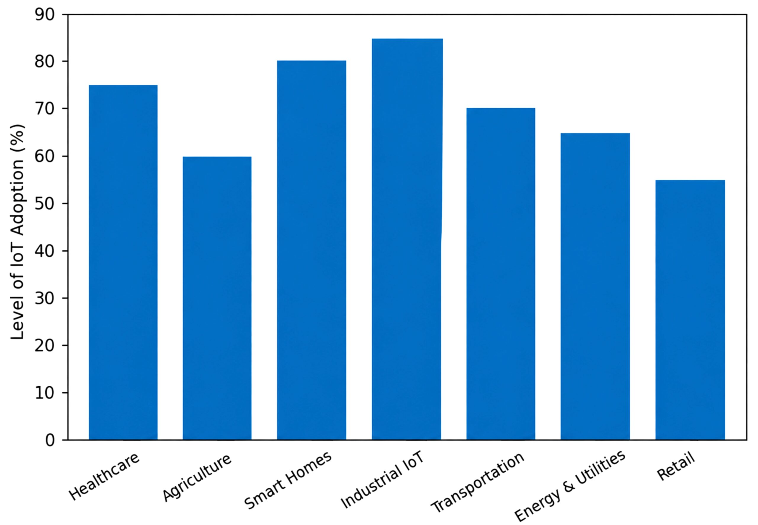
IoT devices are increasingly used across multiple sectors to drive automation and efficiency, as shown in Figure 1. Key applications include smart cities: traffic control, public service management5; agriculture: soil sensing, automated irrigation, crop monitoring7; health monitoring: continuous patient observation, early detection of medical issues8; environmental sciences: continuous data on air quality, water systems, climate conditions6; banking: secure transactions, customer analytics, asset tracking9; and smart manufacturing: automation, real-time production monitoring10.
IoT devices collect continuous data from their physical environment via analog sensors and actuators; these analog signals are converted, filtered, and processed into digital signals that microcontrollers can read. Mixed-signal integrated circuits (MSICs) integrate digital and analog functions on a single chip; this approach enables digital sensors to perform discrete tasks while also allowing high-precision, continuous measurements with analog sensors. These circuits typically include components such as analog-to-digital converters (ADCs), digital-to-analog converters (DACs), and power-management and communication interfaces11. Thoughtful design and integration of these components onto circuits is essential to minimize power consumption without sacrificing accuracy and reliable communication.
Low-power MSIC design presents several challenges. It can be more difficult to leverage clock or power gating methods in analog circuits compared to digital circuits, because some analog blocks have to remain biased or require settling time after being activated. Integrating analog-digital blocks on a single substrate also introduces signal integrity issues12,13,14. Rapid digital switching creates coupling noise that can reduce the accuracy of sensitive analog circuits, such as ADCs. Leakage also occurs in idle states in both domains, which reduces the overall power efficiency. Process scaling additionally introduces challenges because reduced supply voltages limit the analog headroom, while device mismatch can make it more difficult to maintain accuracy across process and voltage variations. Although these challenges are common for general MSICs, they become prevalent in IoT devices because of the strict energy constraints. These effects make it difficult to optimize both low power consumption and high precision in MSICs.
The effectiveness of these architectures also depends on their level of scalability, reliability, and energy efficiency. The primary objective of this paper is to synthesize the latest research on low-power MSIC design and identify future avenues that address current limitations within IoT applications.
Methodology
Google Scholar, IEEE Xplore, and SpringerLink were used to survey literature relevant to low-power MSICs for Internet of Things applications. Searches were conducted using keywords such as “low-power design”, “mixed-signal integrated circuits”, “IoT hardware”, “dynamic voltage and frequency scaling”, “digitally assisted analog”, “charge recycling”, “event-driven circuits”, and “analog-digital co-design”. The literature was restricted to publications from 2005 through 2026.
Studies were considered for this review when they were published between 2005 and 2026, addressed low-power circuit design or MSIC design, contained a technique that was related to IoT or low-power embedded systems, and provided technical information to evaluate the approach. Peer-reviewed journal articles and conference papers were prioritized for collecting evidence. Non-peer-reviewed articles and industry reports were used only for background information and not as primary studies reviewed.
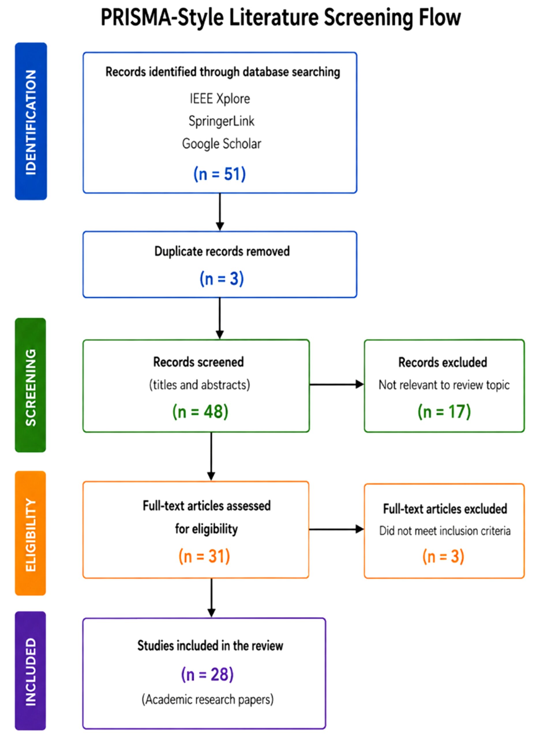
Studies were excluded when they did not address low-power or MSIC design, were not relevant to IoT or low-power embedded systems, or lacked detail or quantitative results. Three duplicate records were removed, which left a total of 48 papers for initial screening. 17 papers were excluded because they were not relevant enough to the review. The remaining 31 were assessed by their full text, and three were excluded because they did not meet the inclusion criteria. Therefore, 28 studies were chosen to be included in the literature review. The included studies were organized based on the technique studied: dynamic voltage and frequency scaling, digitally assisted analog circuits, charge-recycling, event-driven circuits, and analog-digital co-design.
For each study, the following information was extracted: circuit or system architecture, application, supply voltage, power or energy consumption, achieved energy savings, and performance metrics. The studies were then compared to find advantages, limitations, and application areas that were common for each low-power technique. Additional metrics considered in this study are non-power metrics, such as accuracy, noise, linearity, latency, area, reliability, and security, as reported by the source.
This study adopts a thematic research approach to analyze design techniques and challenges, identify common trends, and emphasize future directions. The literature screening process is summarized by using a PRISMA-style flow diagram in Figure 2.
Literature Review
As CMOS technology has progressed from mature to advanced process nodes, digital circuits have excelled due to the increased transistor density. However, this reduces supply voltages from 1.8 V in many 180 nm chips to approximately 0.9-1.0V in many 28nm chips. Consequently, there is significantly less analog headroom voltage, which makes it more difficult to design high-gain amplifiers and analog interfaces while maintaining accuracy and low noise. Therefore, low-power MSIC techniques are adapted to account for this scaling. For example, digitally assisted circuits become very valuable because the digital logic can compensate for the analog limitations, while dynamic voltage and frequency scaling and charge-recycling require more optimization to account for the decreased voltage headroom.
Research has produced a range of fundamental low-power design methods that are principles for IoT systems. Not all of the studies reviewed were developed specifically for IoT applications. Some demonstrate general low-power MSIC techniques that are broadly applicable in embedded systems, while others target IoT-specific areas. In this review, the broader methodologies are evaluated based on their relevance to IoT MSIC design. This paper will focus on the following widely used mixed-signal power reduction methods: dynamic voltage & frequency scaling (DVFS), digitally assisted analog circuits (DAA), charge-recycling, event-driven architecture (EDA), and analog-digital co-design.
Dynamic Voltage & Frequency Scaling
Dynamic voltage and frequency scaling (DVFS) is most commonly employed as a system-level power-saving technique in which the supply voltage and clock frequency are adjusted according to the energy demand. In MSIC IoT systems, DVFS uses chip components such as voltage regulators and digital control units to adjust the parameters. When the system demand is low (low workload or idle), the circuit can operate at a lower supply voltage and lower clock frequency, which lowers power consumption. When high performance is needed, the voltage/frequency is increased to meet the demand. This technique corresponds to the dynamic power equation (1).
Pdynamic is power in watts, ɑ is switching activity, CL is load capacitance, Vdd is supply voltage, and ƒ is clock frequency. DVFS involves reducing Vdd and ƒ to yield a reduction in dynamic power, making DVFS a powerful tool in energy-conservative devices. DVFS is useful in systems with changing workloads because most of the time they operate at a lower frequency and voltage, and only increase these parameters when peak performance is needed.
Research by Ahn et al. proposed a cochlear-implant stimulation front end that reduces wasted energy by only supplying the voltage needed for a pulse15. This system integrates an adaptive dynamic voltage switching (ADVS) block that dynamically adjusts the supply voltage to real-time environmental conditions. Upon receiving the stimulation requirements, the ADVS block dynamically commands the regulator to supply the minimum required voltage during the instantaneous pulse. After testing, results showed up to ~13.5% longer battery life due to ADVS reducing wasted energy.
In a study by Zidar et al., the authors evaluated DVFS in ultra-low-power embedded systems16. However, instead of examining whole-system power, they focused on individual tasks that require heavy processing; by doing this, they were able to assess the direct effect of DVFS, independent of system architecture. The authors utilized a DC-DC programmable voltage regulator, which allowed them to track the minimum frequency and voltage at which the chip still works reliably. Based on these measurements, an exponential model for stable voltage scaling relative to operating frequency was proposed. Rather than relying on conservative power guardbands, the model determines the lowest supply voltage that will reliably support the chosen clock frequency. This approach allows low-power embedded systems to minimize energy consumption while maintaining stable operation, and this can be applied to many battery-powered embedded systems beyond the chip surveyed in the study. The paper concluded that DVFS resulted in energy savings of 27.74% to 47.74% compared to running at a fixed V-F level.
While these studies highlight the advantages of utilizing adaptive voltage scaling in biomedical stimulation and embedded systems, DVFS can also be applied directly to MSICs. Chou et al. demonstrated an embedded dynamic voltage scaling system in a 55-nm CMOS mixed-signal system that used a 12-bit video DAC and a single-inductor dual-output (SIDO) converter, which allowed the analog and digital blocks to receive independently controlled voltages17. The system acquired an 11.5% improvement in power efficiency in the DVS mode; the DAC also achieved 69.88 dB SFDR with a 1 V swing and 1 MHz input frequency. The system demonstrated that voltage scaling can be implemented while meeting the analog performance.
However, DVFS does not always provide an energy benefit because manipulating voltage and frequency introduces transition overhead. Park et al. analyzed the energy and timing overhead that arose with DVS transitions in a processor18. The authors found that a DVS transition causes additional energy consumption from the voltage regulator and inductor losses. Using their analytical model and LTSPICE simulations, they showed that the transition overhead varies depending on the voltage and frequency levels being changed. For example, transition overheads varied from 14.7 µJ to 73.7 µJ across different voltage changes. They concluded that there was a break-even time where the system must remain at the new voltage-frequency points for the energy saved from DVFS to exceed the energy consumed during transitions.
This limitation is specifically relevant to IoT systems with short or frequently changing workloads. If a sensor node constantly switches between active and idle states before remaining at the voltage-frequency point for longer than the break-even time, the energy saved with DVFS implementation will be ineffective. Consequently, DVFS is most beneficial when the workload contains long operating periods.
Across the analyzed research, IoT-based DVFS is implemented in two primary methods: event- and task-driven DVFS. Event-driven frameworks tightly coordinate voltage scaling to short pulses and prioritize instantaneous voltage accuracy and fast regulator pulses. This style minimizes energy when the circuit is idle, making it highly applicable to duty-cycled IoT sensor nodes. However, task-level DVFS frameworks that operate at varying time lengths change the voltage and frequency to optimize average energy per task. This design is useful for computationally intensive tasks, which makes it more applicable for IoT edge processors that execute changing workloads.
These results underscore DVFS’s tradeoff between low idle power and computational strength. DVFS is most effective in IoT architectures where workload timing can be predicted or when devices perform continuous computation to prevent transition overhead.
For example, a soil-moisture sensor that only wakes up a few times per hour to sample data will have long idle states. During these intervals, the processor can operate at a lower voltage and frequency, and then increase when computation or transmission of data is required. Conversely, IoT edge processors experience large changes in computational demand; the ability to modulate the energy spent with task-level DVFS will significantly help to maintain performance.
Digitally Assisted Analog Circuits
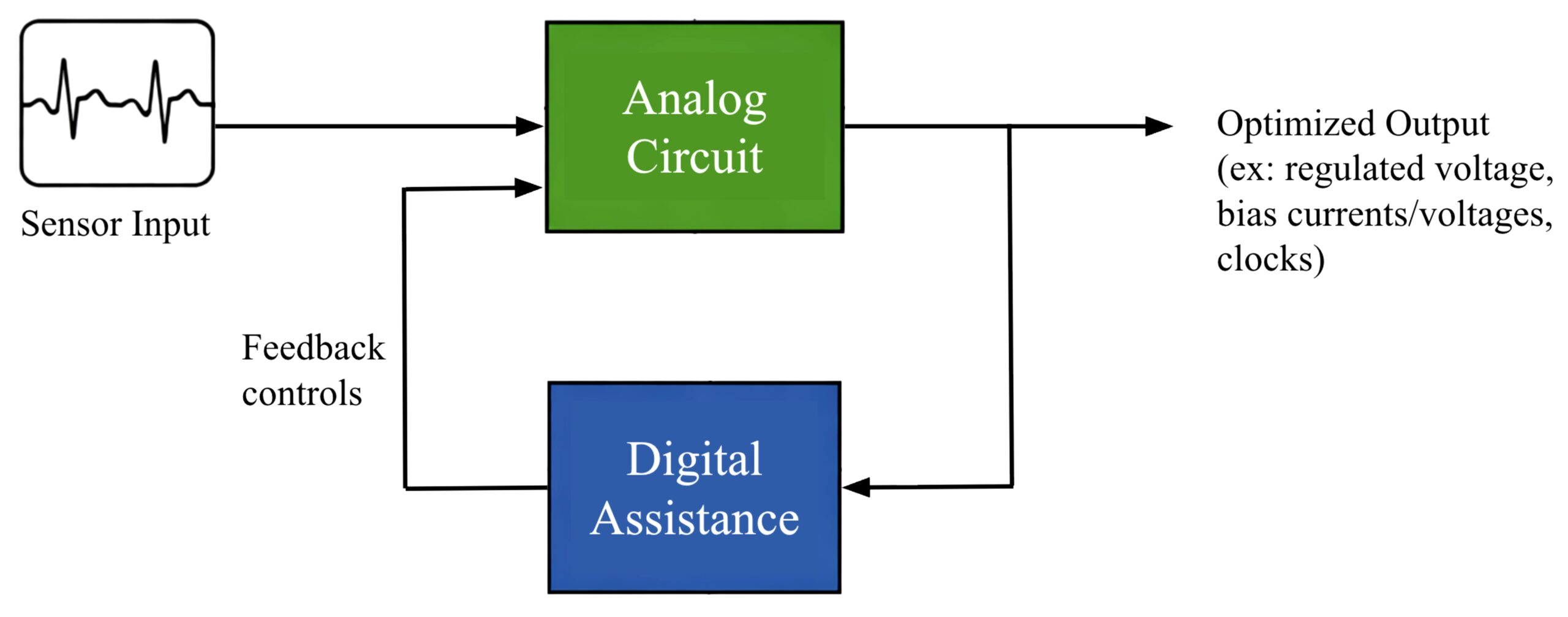
Digitally assisted analog (DAA) systems utilize digital control circuits to enhance the performance of analog blocks. As detailed in a review by Huang et al., DAA architectures leverage digital assistance to improve the accuracy and efficiency of analog circuits without using a fully digital implementation (traditional DAA architecture illustrated in Figure 3)19. In low-dropout regulators (LDOs), for example, digital components can adjust biasing dynamically, allowing high performance under heavy loads. Compared to traditional analog designs, DAA techniques allow more control over power consumption and faster response times, which makes them important for energy-sensitive applications.
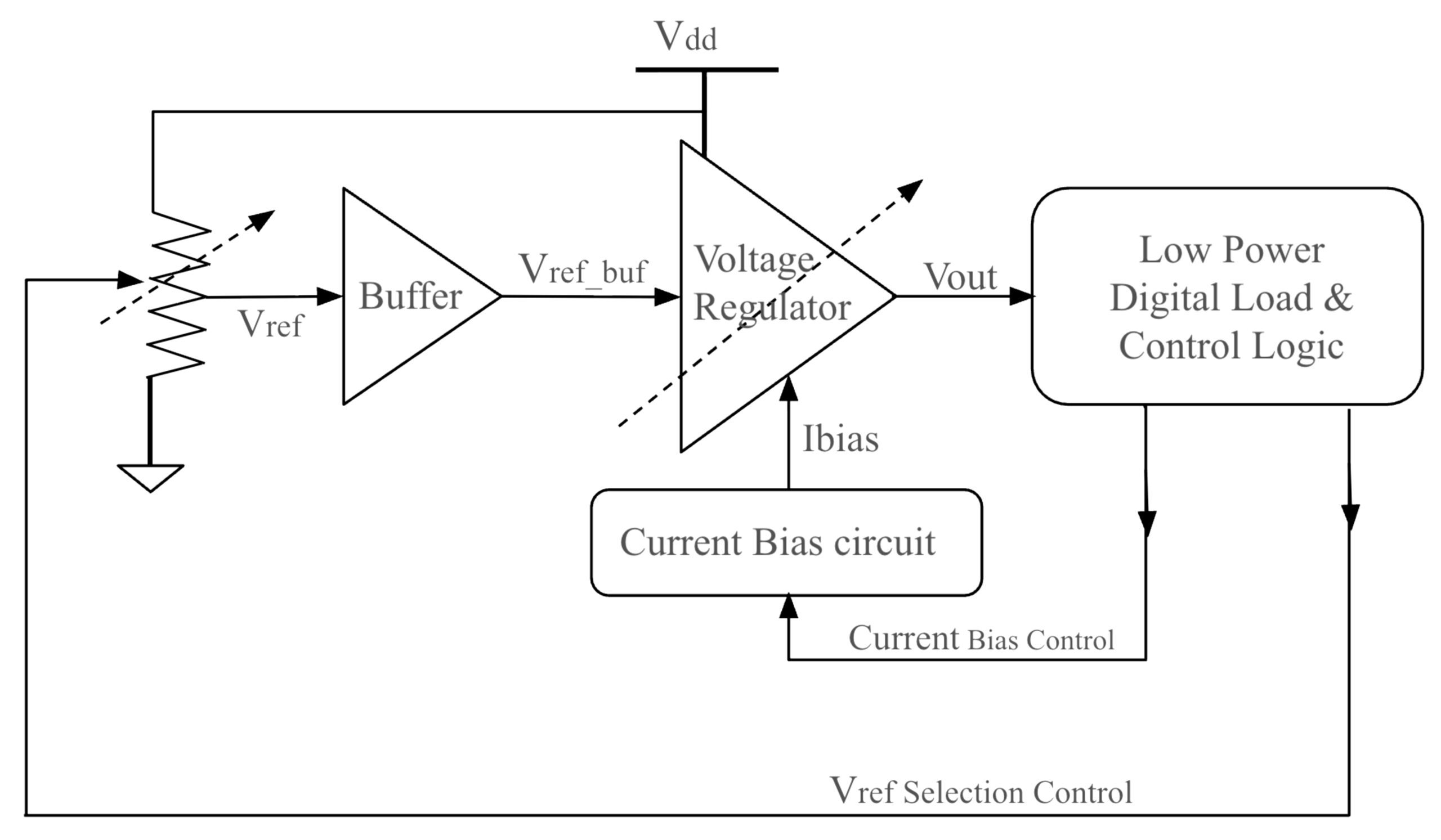
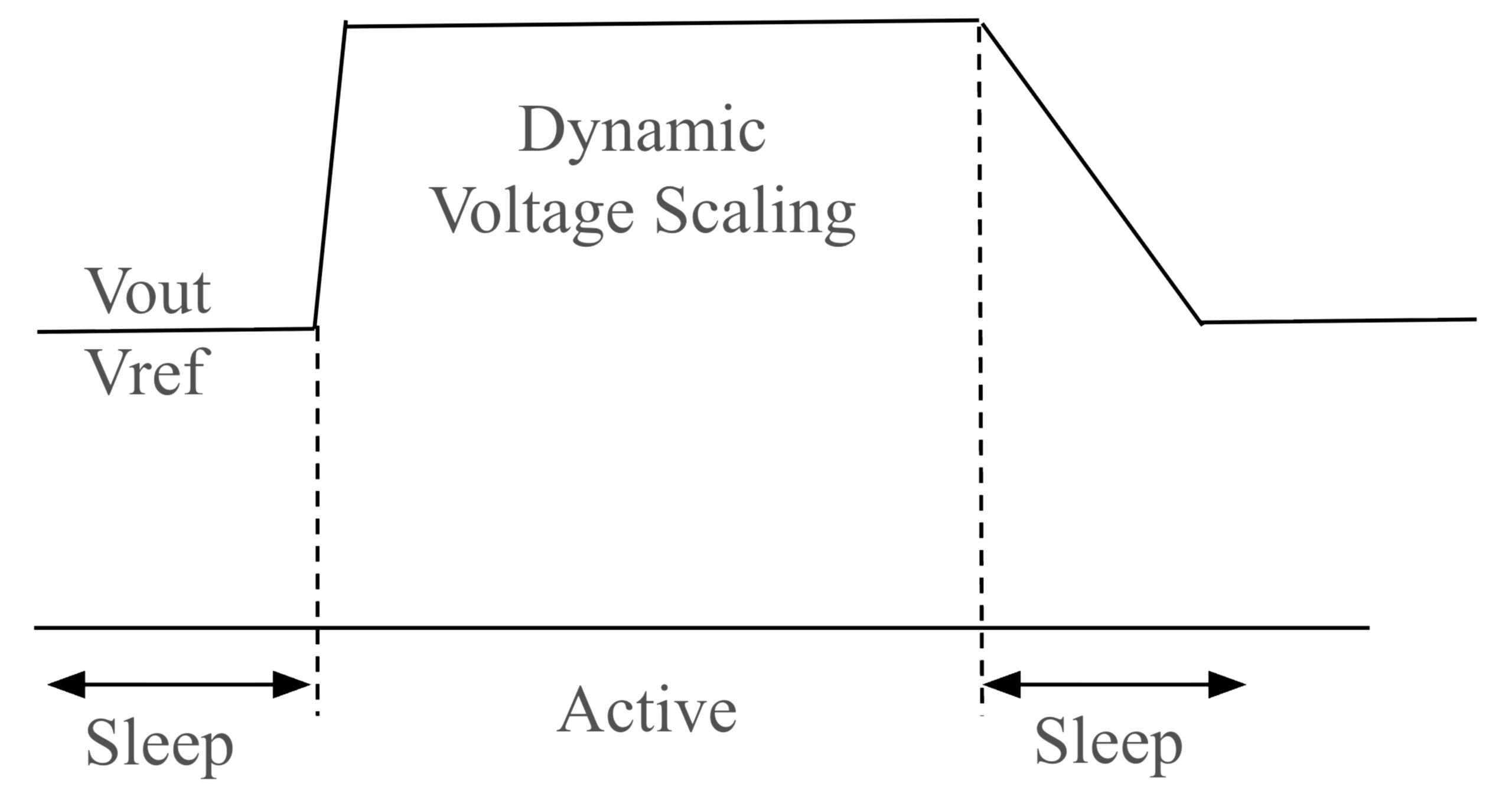
In a study by Yan Lu, the primary aim was to develop an LDO that can operate efficiently under changing power demands20. Figure 4(a) shows the proposed design, which incorporates a digitally assisted control loop to optimize short response and reduce unnecessary current during low duty-cycle operation. Based on the workload requirements, the digital control logic modulates Vref (voltage reference) and Ibias (current bias) of the voltage regulator. When the performance requirement increases, the control logic boosts the Vref by dynamically scaling the voltage, and the regulator, in turn, increases the Vout to track the Vref. As shown in Figure 4(b), once the high-performance requirements are achieved, the logic dynamically scales down the Vref and Vout. Thus, the scheme transitions between sleep and active modes and achieves low-power and performance requirements.
Results highlight the achieved low current (28 µA) and low sleep current (45 nA). This demonstrates digitally assisted circuits’ ability to balance energy efficiency with performance and maintain stable voltage regulation.
DAA techniques have also been applied to low-power ADC architectures. Xu et al. developed a digitally calibrated 10-bit SAR ADC array for applications that require small area and low power21. The design consisted of 256 ADCs, and digital calibration was used to compensate for capacitor mismatch in the CMOS fabrication. The calibration permitted the authors to use small-sized capacitors in the SAR ADC while maintaining conversion accuracy. Along with reducing the area required for each ADC, the results showed that the effective number of bits (ENOB) improved as well. This demonstrates how digital assistance can reduce the analog hardware needs of an ADC while increasing performance with the help of digital calibration. The digital correction additionally helped scale area efficiency.
The reviewed examples demonstrate different applications of DAA in low-power mixed-signal systems. The LDO design uses digital control to dynamically reduce analog current during periods of low processing, while the SAR ADC uses digital calibration to compensate for analog mismatches and reduce the size of circuitry. Overall, DAA can be used dynamically to control analog power or reduce the hardware required to achieve performance requirements. In low-power IoT sensor nodes, analog frameworks often have the highest energy consumption during both active and idle states. In event-driven sensors, such as environmental monitors and wearable technologies, the ability to decrease bias currents while maintaining fast wake-up behavior is essential to foster long battery life.
Charge-Recycling
Charge-recycling is a technique used in switched capacitor or capacitive-DAC circuits (e.g., SAR ADCs) and other mixed-signal blocks. Rather than dissipating the charge stored on sampling capacitors to ground after each conversion step, charge-recycling reuses and redistributes previously stored charge through digitally controlled switching steps, thereby reducing the energy drawn from the supply.
Charge-recycling introduces an analog circuit that is controlled by digital logic (SAR state machines, clocks). Since the architecture involves the co-design of analog energy storage and digital sequencing, this technique is classified as a mixed-signal methodology.
Figure 5 shows a switched-capacitor charge-recycling circuit using two capacitors that operate in a two-phase cycle. In phase-1, the first switch (S1) closes while the second switch (S2) remains open, allowing C1 to charge to VIN. In phase-2, S1 opens, and S2 closes, letting C1 transfer charge to C2 until their charges balance. After C2 supplies energy to the load, C1 partially replenishes C2, and finally S1 closes again to recharge C1 from VIN, repeating the cycle.
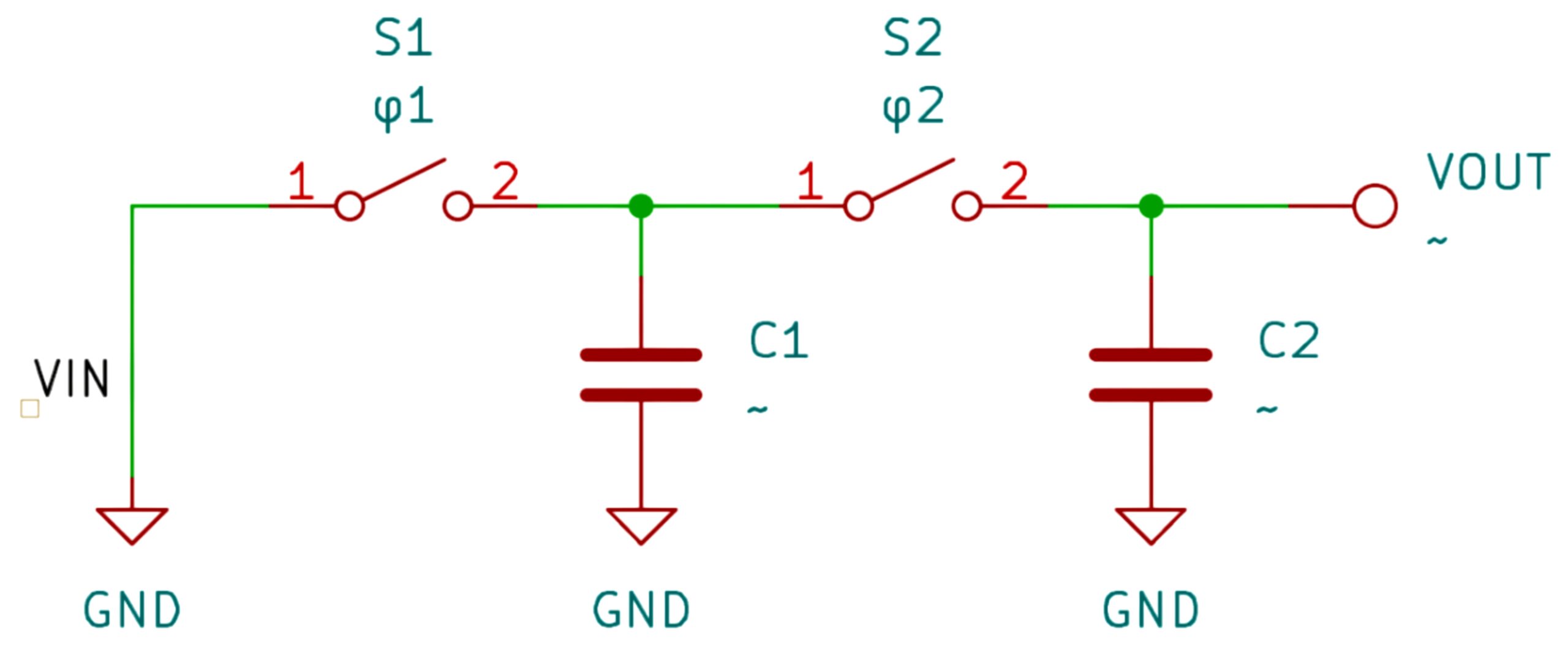
This switched-capacitor design conserves energy by reusing stored charge rather than drawing it directly from the source for every cycle. Since C1 acts as an intermediate voltage source, transferring part of its stored charge to partially replenish C2, this reduces the amount of current that must be drawn from VIN. This reduces the energy drawn from the supply compared with conventional charge-dissipative switching. By timing the switches through digital logic, the circuit ensures that C1 is recharged only when needed, and C2 receives energy efficiently from C1. In this way, the circuit recycles energy between capacitors and the load, improving overall efficiency compared to directly powering the load from the voltage source each time22.
Ginsburg et al. apply charge-recycling techniques to the capacitive DAC of a SAR ADC23. Their switching energy method reduces the average switching energy of the capacitor array by 37% compared with traditional switching.
Charge-recycling can also be extended beyond individual ADC circuits to architectures considering power management. Blutman et al. demonstrated a 40-nm CMOS low-power microcontroller that used charge-recycling through voltage stacking24. Voltage stacking involves arranging power domains so that energy can be reused between the domains rather than have each domain draw power independently. The system additionally incorporated a switched-capacitor voltage regulator to provide an intermediate voltage. The converter achieved a power-conversion efficiency of 96%, while the system reduced the converter area by a factor of 2.6 and supply noise by 3.4 dB.
Across IoT MSIC designs, charge-recycling is a frequently employed strategy to reduce the energy usage at both the circuit and system levels. This study evaluates the effectiveness of charge-recycling in reducing conversion energy and also improving power-conversion efficiency. This technique is not limited to a specific mixed-signal block, but should instead be used to store energy that would otherwise be discarded during switching or voltage conversion.
These results indicate that charge-recycling is most advantageous for duty-cycled IoT nodes, in which a large portion of total energy is spent charging and discharging capacitors. Charge-recycling addresses this issue by implementing internal charge redistribution and significantly lowering the energy consumption. Charge-recycling is especially beneficial in sensor nodes that perform continuous analog-to-digital conversions, such as temperature systems. Because capacitive-DAC conversion requires charging and discharging of capacitors, recycling the charge lowers the energy needed for each shift. This significantly extends the battery life of devices that perform thousands of sensing operations in their lifespan.
Despite the benefits, charge-recycling introduces additional design complexity. Implementing this technique requires extra switching paths and digital control logic, and careful timing is needed to ensure that the charge is distributed without reducing conversion accuracy. With these additions come increased circuit area and design complexity, which are important factors in IoT devices. Although the reviewed studies demonstrate strong energy-saving results through charge-recycling, they do not mention the additional area or control management compared to traditional capacitive DACs. Ultimately, designers have to balance the reduced energy consumption with the implementation complexity when selecting charge-recycling architectures.
Event-Driven Architecture
Event-driven architecture (EDA) in low-power design is a method in which a system remains in an “idle” state until an event occurs (e.g., a sensor crossing a threshold). Ultra-low-power analog comparators and event-driven ADCs continuously monitor the sensor inputs while the rest of the system operates in the “idle” state. EDA is a system-level methodology that is performed with low-powered mixed-signal circuit blocks. When such an event is detected, the circuit “wakes up” and performs more power-consuming processing. This method ensures the circuit is only enabled during relevant events.
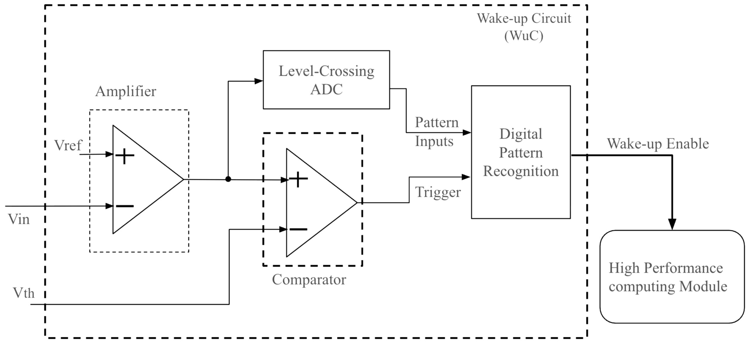
In Figure 6, Rovere et al. present an always-on, event-driven wake-up circuit (WuC) that continuously monitors inputs while the rest of the system remains completely powered off25. When the WuC detects an event, it activates stronger analog and digital blocks to perform computation. The WuC is able to perform these actions with the integration of a level-crossing ADC (LC-ADC) with a digital logic classifier that recognizes predefined signal patterns. When the LC-ADC detects a threshold crossing, it triggers the classifier, and if the pattern matches, it wakes up the rest of the system. Their prototype achieves classification of real-world events (e.g., hand movement recognition with the use of an accelerometer). This design consumes just 2.2 µW at 1V while supporting signals up to 2.6 kHz. Besides ultra-low power, this design reports significantly less switching losses because the LC-ADC provides analog preprocessing without a continuous clock.
Zhang et al. present an ultra-low-power, event-driven ADC for wearable electrocardiogram sensors26. Instead of utilizing traditional ADCs that continuously sample, the designed ADC only activates when the input signal crosses a threshold. This detection simultaneously starts digitization and detection algorithms, so cardiac events are processed without continuous monitoring. The proposed event-driven approach allows the rest of the system to remain mostly idle during quiet periods, which drastically reduces power consumption. Their prototype operates at just 300 mV and 220 nW, while the simulated QRS detector achieves 97.63-97.76% sensitivity and 97.33-98.59% positive prediction. By integrating the detection logic directly with event-triggered detection, this design also reduces switching losses and unnecessary ADC activity.
As highlighted in the analyzed research, event-driven low-power architectures are most effective in IoT systems where signal activity is low. Rather than continuously clocking all subsystems, event-driven architectures concentrate power consumption on single instances of information, allowing circuits to remain in idle states for the majority of runtime. Typical application domains include those where long-lifetime sensing is required: platforms such as wearable health monitors, implantable devices, and wildlife monitoring nodes.
Wearable electrocardiogram (ECG) monitors provide an example where this low-power strategy is a suitable approach. Instead of continuously activating the ADC and digital processor, the event-driven system remains in an ultra-low-power state and only wakes when an important signal is detected. Similarly, security and other monitoring sensors remain idle for long periods, only briefly activate for unusual events, and event-driven approaches to these devices significantly reduce average energy consumption.
Despite the advantages, event-driven architectures have many design trade-offs. Their performance heavily depends on reliable threshold detection, since circuit noise and comparator offset can cause false wake-ups or events to be missed. Because the system is idle until an event is detected, there is also latency between when the system wakes up and when processing begins. In applications where events occur frequently, repeated wake-ups reduce the energy savings compared to continuously operating systems. Therefore, event-driven techniques are most effective in systems with infrequent and distinct events.
Analog-Digital Co-design
Analog-digital co-design optimization frameworks model the interactions between analog and digital blocks and involve the simultaneous optimization between these domains. This method allows system energy, area, and accuracy to be co-optimized, which is crucial in IoT applications. By jointly optimizing analog currents and digital voltage/frequency, the framework minimizes total energy while ensuring constraints are maintained.
As highlighted by the analog-digital co-design workflow in Figure 7, co-design also applies to individual circuit blocks by treating the analog and digital units as one system. Rather than designing the components independently, parameters such as bias currents, digital supply voltage, clock frequency, and signal processing algorithms are jointly optimized so that they satisfy system-level parameters such as power consumption and latency. For broader co-design, this optimization can also extend to the interaction between sensors, ADCs, bandwidth, and digital computation. This approach is valuable in IoT systems, where performance in one domain can influence the energy consumption in the other.
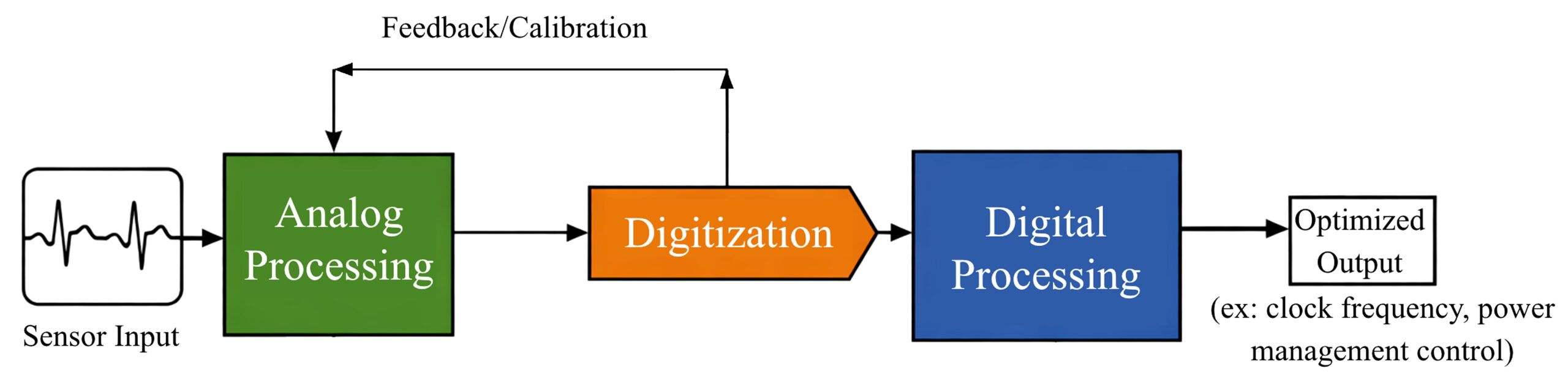
An example of this workflow for IoT-specific implementation is presented by Shatta et al., where the authors propose a feature-to-classifier mixed-signal co-design framework for flexible, wearable healthcare devices27. They aimed to address a concern with existing systems: prior works optimized the digital classifier, even though feature extraction and ADCs were the majority of the hardware cost (feature extraction accounted for ~46% of area, and ADCs ~51% of the system power). To overcome this, the authors designed a fully mixed-signal chain consisting of custom analog feature extractors, a low-resolution SAR ADC, and an MLP on FlexIC chips. By performing all computations in the analog domain, the framework reduced the requirements of the digital block while maintaining accuracy.
A broader analog-digital co-design approach was demonstrated by Datta et al. through their P2M framework for TinyML systems28. Rather than optimizing purely machine learning stages, such as feature extraction or classification, the framework additionally optimizes sensing, analog computation, ADC conversion, data transfer, and digital computation. Their approach also included circuit-level constraints in the design process, which allowed the hardware and neural network to be optimized altogether. The system-level approach reported an approximate reduction in data-transfer bandwidth and ADC conversions by a factor of 21, and a reduction in energy-delay by a factor of 11, without a significant loss in accuracy. These results highlighted that the optimization of analog sensing and digital processing domains together reduced the energy spent on data transfer and conversion.
Through the reviewed literature, it is demonstrated that there are two levels of analog-digital co-design. The first focuses on the mixed-signal process, showing how analog feature extraction and conversion can reduce the demands for later digital classification. In contrast, broader frameworks that target the pathway from sensing to computation incorporate circuit constraints in algorithm logic. Therefore, co-design extends to jointly optimizing analog and digital blocks for energy, area, accuracy, latency, and bandwidth.
Comparison and Combination of Low-Power Mixed-Signal IC Techniques
Tables 1a and 1b show that no single low-power MSIC technique consistently minimizes all forms of energy consumption. The reviewed techniques target different components of the energy budget of a system: DVFS addresses computational energy, DAA addresses analog bias and power management, charge-recycling addresses switching and conversion energy, event-driven architectures minimize unnecessary activity during inactive periods, and analog-digital co-design jointly optimizes interactions across these domains. Therefore, the most appropriate technique depends on where the strongest source of energy consumption originates and the specific characteristics of the IoT system rather than on a single low-power approach.
| Technique | Energy/efficiency (application; evaluation) | |
| DVFS16 | 27.74-47.74% lower energy vs. fixed V-F (embedded processor; measured) | |
| DVS17 | 11.5% power-efficiency improvement in DVS mode (low-power SoC; measured) | |
| DAA20 | (low-power LDO; simulated) | |
| Charge recycling23 | 37% reduction in average DAC switching energy vs. usual switching (SAR ADC; simulated) | |
| Charge recycling24 | 96% power-conversion efficiency (power converter; measured) | |
| Event-driven25 | (IoT wake-up sensing; measured) | |
| Event-driven26 | (Wearable ECG; measured + simulated) | |
| Analog-digital co-design27 | (Wearable sensing; simulated) | |
| Analog-digital co-design28 | ~11x lower EDP (TinyML sensing; experimental) |
| Technique – cited work | Power | Wake- up/latency | Vdd (V) | Process node | Bandwidth/ resolution | |
| DVFS – Zidar et al. | 1.94 V | |||||
| DVS – Chou et al. | 55 nm CMOS | 12-bit DAC, 1 MHz | ||||
| DAA – Lu | 28 μA active; 45 nA idle | 11 V/μs tracking | 65 nm CMOS | |||
| Charge recycling – Ginsburg & Chandrakasan | 0.18 μm CMOS | 10-bit SAR ADC | ||||
| Charge recycling – Blutman et al. | 40 nm CMOS | |||||
| Event-driven – Rovere et al. | 2.2 μW | 1 V | 130 nm CMOS | 2.6 kHz | ||
| Event-driven – Zhang & Lian | 220 nW | 300 mV | 0.13 μm CMOS | |||
| Analog-digital co-design – Shatta et al. | 20.3 mW | <20 ms | 3 V | FlexIC Gen-3 IGZO TFT | 4-bit ADC; 10 kHz | |
| Analog-digital co-design – Datta et al. | ~21x lower data-transfer/ADC activity |
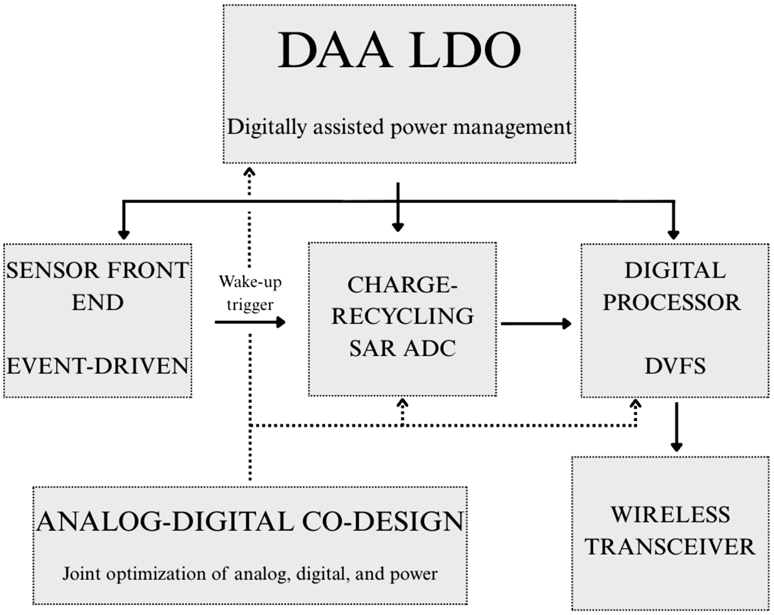
Since each technique targets different sources of energy consumption, combining techniques is also a viable methodology that may provide greater system-level savings. As a thought experiment, consider a battery-powered environmental sensing node that monitors sound and temperature signals and transmits data when a defined event occurs. The architecture in Figure 8 utilizes all five discussed low-power MSIC techniques: an event-driven front end that keeps the system in ultra-low-power mode and only wakes the system when a threshold crossing is detected; a DAA LDO that regulates voltage across varying loads of the different blocks; a charge-recycling SAR ADC that reduces conversion energy; DVFS adjusts the digital processor according to the workload demand; and analog-digital co-design is applied across the analog, digital, and power domains to jointly optimize energy consumption and performance. To provide a hypothetical energy budget, assume 0.5 μJ for event detection, 1 μJ for regulation, 2 μJ for ADC conversion, 5 μJ for processing, and 20 μJ for transmission, giving approximately 28.5 μJ per event.
Discussion
In this study, low-power design in IoT MSICs, through mixed-signal techniques such as DVFS, DAA circuits, charge-recycling, event-driven architectures, and analog-digital co-design, is explored. The findings highlight that an approach combining circuit-level and system-level low-power strategies is necessary to meet the energy and performance demands of modern IoT devices.
Although the low-power techniques target energy efficiency, they also affect other important mixed-signal metrics. Circuits operating at lower supply voltages are increasingly susceptible to timing failures and soft errors as transistor form-factor scales. In analog blocks, reduced supply voltage reduces the voltage headroom and signal amplitude, which makes it difficult to maintain high linearity and dynamic range while the sensitivity to noise and aging is increasing. Additionally, techniques such as charge-recycling digitally assisted analog circuits can reduce power consumption, but they may require complex switching networks, logic, and more chip area. In low-power design, it is also essential to understand the induced security risks. By scaling voltage and frequency, circuit timing and power consumption may increase the susceptibility to side-channel attacks. In MSIC design, interfaces are vulnerable to noise injections and signal manipulation because countermeasures are too power-hungry to implement. Hence, reliability, efficiency, and security should be considered along with low-power methodologies to ensure IoT devices can sustain long-term operations.
Despite significant advances in low-power MSIC design, several research challenges remain. Improvement is required for verification frameworks for analog-digital co-design architectures that can model interactions between analog and digital blocks in early design periods. Additional research is needed to reduce wake-up energy and false wake-ups caused by detected errors in event-driven architectures, all while maintaining ultra-low idle power. Charge-recycling techniques need to be more scalable for implementations that minimize switching complexity and chip area for IoT devices where cost is a high priority. More broadly, future design methodologies should jointly optimize power consumption, accuracy, reliability, and cost across complete mixed-signal systems rather than optimizing individual blocks separately.
Beyond individual circuit-level techniques, future system-level research should focus on low-power architectures. Industry research on multi-die chiplet architectures can potentially help future MSIC designs to further achieve lower levels of platform or system power consumption by decoupling high-computing digital and analog/mixed-signal circuits onto different dies. Independent per-die DVFS, power gating, and event-driven techniques will boost performance and allow each die to be manufactured with its own process node to achieve overall power-performance-area enhancements. These trends indicate that future low-power IoT devices will be increasingly co-optimized analog-digital systems that minimize lifetime energy consumption rather than single low-power circuit techniques.
Conclusion
This paper discusses low-power MSIC design techniques and how these methods are essential for meeting the energy constraints of modern IoT systems. The findings illustrate that techniques such as DVFS, digitally assisted analog circuits, charge-recycling, event-driven architecture, and analog-digital co-design each have different ways to reduce power consumption while maintaining accuracy and performance. However, limitations stress the need for different, adaptive design approaches. Because each technique targets different sources of energy consumption, no single method is sufficient for all low-power MSIC IoT applications. The paper reinforces that a holistic approach combining techniques can improve overall energy efficiency while maintaining performance, accuracy, and adhering to implementation constraints. Future research should focus on predictive MSIC design optimization frameworks, extended charge-recycling strategies, and multi-die architectures. As IoT systems continue to expand into different sectors and increase in autonomy, advances in low-power MSIC design will play a crucial role in creating sustainable, reliable computing.
References
- MarketsandMarkets™. IoT Market worth $865.20 billion by 2030. https://www.marketsandmarkets.com/PressReleases/iot-m2m.asp, 2025. [↩]
- S. Sinha, State of IoT 2025: Number of connected IoT devices growing 14% to 21.1 billion globally. https://iot-analytics.com/number-connected-iot-devices/, 2025. [↩]
- M. Haras, N. Ahmed, T. Skotnicki. Further IoT market expansion owing to innovative thermal energy harvesting. 2022 IEEE 16th International Conference on Solid-State & Integrated Circuit Technology (ICSICT). 2022, pg. 1-4, https://doi.org/10.1109/ICSICT55466.2022.9963142. [↩]
- Y. Wu, R. Brito, W. Choi, C. Lam, M. Wong, S. Sin. IoT cloud-edge reconfigurable mixed-signal smart meter platform for arc fault detection. IEEE Internet of Things Journal. Vol. 10, pg. 1682-1695, 2023, https://doi.org/10.1109/JIOT.2022.3210220. [↩]
- A. Zanella, N. Bui, A. Castellani, L. Vangelista, M. Zorzi. Internet of Things for smart cities. IEEE Internet of Things Journal. Vol. 1, pg. 22-32, 2014, https://doi.org/10.1109/JIOT.2014.2306328. [↩] [↩]
- A. Rehman, A. Abbasi, N. Islam, Z. A. Shaikh. A review of wireless sensors and networks’ applications in agriculture. Computer Standards & Interfaces. Vol. 36, pg. 263-270, 2014, https://doi.org/10.1016/j.csi.2011.03.004. [↩] [↩]
- S. Wolfert, L. Ge, C. Verdouw, M. Bogaardt. Big data in smart farming—a review. Agricultural Systems. Vol. 153, pg. 69-80, 2017, https://doi.org/10.1016/j.agsy.2017.01.023. [↩]
- S. M. Islam, D. Kwak, M. H. Kabir, M. Hossain, K. Kwak. The Internet of Things for health care: a comprehensive survey. IEEE Access. Vol. 3, pg. 678-708, 2015, https://doi.org/10.1109/ACCESS.2015.2437951. [↩]
- S. Madakam, R. Ramaswamy, S. Tripathi. Internet of Things (IoT): a literature review. Journal of Computer and Communications. Vol. 3, pg. 164-173, 2015, http://www.scirp.org/journal/PaperInformation.aspx?PaperID=56616&#abstract. [↩]
- H. Lasi, P. Fettke, H. Kemper, T. Feld. Industry 4.0. Business & Information Systems Engineering. Vol. 6, pg. 239-242, 2014, https://doi.org/10.1007/s12599-014-0334-4. [↩]
- J. Zhang, T. Sun, Z. Huang, W. Tao, N. Wang, L. Tian, Y. Zhu, H Wang. The design of a low-power pipelined ADC for IoT applications. Sensors. Vol. 25, 1343, 2025, https://doi.org/10.3390/s25051343. [↩]
- M. M. Alam, S. Chowdhury, B. Park, D. Munzer, N. Maghari, M. Tehranipoor, D. Forte. Challenges and opportunities in analog and mixed signal (AMS) integrated circuit (IC) security. Journal of Hardware and Systems Security. Vol. 2, pg. 15-32, 2018, https://doi.org/10.1007/s41635-017-0024-z. [↩]
- T. C. S., N. Shanmugasundaram. Clock gating techniques: an overview. 2018 Conference on Emerging Devices and Smart Systems (ICEDSS). 2018, https://doi.org/10.1109/ICEDSS.2018.8544281. [↩]
- P. Verma, A. Noor, A. K. Sharma, S. K. V. Power gating and its repercussions—a review. 2016 IEEE 1st International Conference on Power Electronics, Intelligent Control and Energy Systems (ICPEICES). 2017, https://doi.org/10.1109/ICPEICES.2016.7853208. [↩]
- W. Ahn, K. Nguyen, H. Lee, K. S. Min, S. Ha, M. Je. An energy-efficient stimulation system based on adaptive dynamic voltage switching control for cochlear implants. IEEE Transactions on Biomedical Circuits and Systems. Vol. 19, pg. 803-814, 2025, https://doi.org/10.1109/TBCAS.2024.3497585. [↩]
- J. Zidar, T. Matic, I. Aleksi, Z. Hocenski. Dynamic voltage and frequency scaling as a method for reducing energy consumption in ultra-low-power embedded systems. Electronics. Vol. 13, 826, 2024, https://doi.org/10.3390/electronics13050826. [↩] [↩]
- Chou, W. S., Huang, T. C., Lee, Y. H., Yang, Y. Y., Su, Y. P., Chen, K.-H., Huang, C. C., Lin, Y. H., Lee, C. C., Wen, K.-A., Hsu, Y. C., Peng, Y. C., Hsueh, F. L. An embedded Dynamic Voltage Scaling (DVS) system through 55 nm Single-Inductor Dual-Output (SIDO) switching converter for 12-bit video digital-to-analog converter. IEEE Journal of Solid-State Circuits. Vol. 47, pg. 1568-1584, 2012, https://doi.org/10.1109/JSSC.2012.2191331. [↩] [↩]
- J. Park, D. Shin, N. Chang, M. Pedram. Accurate modeling and calculation of delay and energy overheads of dynamic voltage scaling in modern high-performance microprocessors. Proceedings of the 2010 International Symposium on Low Power Electronics and Design (ISLPED). pg. 419-424, 2010, https://doi.org/10.1145/1840845.1840938. [↩]
- M. Huang, Y. Lu, R. P. Martins. Review of analog-assisted-digital and digital-assisted-analog low dropout regulators. IEEE Transactions on Circuits and Systems II: Express Briefs. Vol. 68, pg. 24-29, 2021, https://doi.org/10.1109/TCSII.2020.3040393. [↩]
- Y. Lu. Digitally assisted low dropout regulator design for low duty cycle IoT applications. 2016 IEEE Asia Pacific Conference on Circuits and Systems (APCCAS). 2017, https://doi.org/10.1109/APCCAS.2016.7803888. [↩] [↩] [↩]
- R. Xu, B. Liu, J. Yuan. Digitally calibrated 768-kS/s 10-b minimum-size SAR ADC array with dithering. IEEE Journal of Solid-State Circuits. Vol. 47, pg. 2129-2140, 2012, https://doi.org/10.1109/JSSC.2012.2198350. [↩]
- D. Ma, R. Bondade. Reconfigurable switched-capacitor power converters. New York, NY, NY: Springer. 2013. [↩] [↩]
- B.P. Ginsburg, A.P. Chandrakasan. An energy-efficient charge recycling approach for a SAR converter with capacitive DAC. 2005 IEEE International Symposium on Circuits and Systems. 2005, https://doi.org/10.1109/ISCAS.2005.1464555. [↩] [↩]
- K. Blutman, A. Kapoor, A. Majumdar, J. G. Martinez, J. Echeverri. L. Sevat, A. P. van der Wel, H. Fatemi, K. A. A. Makinwa, J. Pineda de Gyvez. A Low-Power Microcontroller in a 40-nm CMOS Using Charge Recycling. IEEE Journal of Solid-State Circuits. Vol. 52, pg. 950-960, 2017, https://doi.org/10.1109/JSSC.2016.2637003. [↩] [↩]
- G. Rovere, S. Fateh, L. Benini. A 2.2- μW cognitive always-on wake-up circuit for event-driven duty-cycling of IoT sensor nodes. IEEE Journal on Emerging and Selected Topics in Circuits and Systems. Vol. 8, pg. 543-554, 2018, https://doi.org/10.1109/JETCAS.2018.2828505. [↩] [↩] [↩]
- X. Zhang, Y. Lian. A 300-mV 220-nW event-driven ADC with real-time QRS detection for wearable ECG sensors. IEEE Transactions on Biomedical Circuits and Systems. Vol. 8, pg. 834-843, 2014, https://doi.org/10.1109/TBCAS.2013.2296942. [↩] [↩]
- M. Shatta, K. Balaskas, P. C. L. Duarte, G. Panagopoulos, M. B. Tahoori, G. Zervakis. Invited paper: feature-to-classifier co-design for mixed-signal smart flexible wearables for healthcare at the extreme edge. 2025 IEEE/ACM International Conference On Computer Aided Design (ICCAD). 2025, https://doi.org/10.1109/ICCAD66269.2025.11240680. [↩] [↩]
- G. Datta, S. Kundu, Z. Yin, R. T. Lakkireddy, J. Mathai, A. P. Jacob, P. A. Beerel, A. R. Jaiswal. A processing-in-pixel-in-memory paradigm for resource-constrained TinyML applications. Sci Rep. Vol. 12, 14396, 2022, https://doi.org/10.1038/s41598-022-17934-1. [↩] [↩]